
 English
  Español


When selecting a payment Java Card for a dual-interface banking project, base the decision on the overall payment architecture. The card must support the required contact and contactless protocols, payment applications, encryption features, the GlobalPlatform environment, personalized data, and target certification configurations, while ensuring consistent transaction behavior across both interfaces.
We recommend following this selection sequence:
Payment solution → Applet architecture → Dual-interface support → Storage requirements → Encryption and security → Transaction performance → Certification and production validation
Therefore, the right chip is not simply the fastest or highest-capacity Java Card, but a platform that can reliably run the required banking applications through both contact and contactless channels. We will explain each of these points in detail below.
Selecting a Payment Java Card Based on Payment Applications and Dual-Interface Architecture
Dual-interface payment Java cards integrate two communication environments into a single credential. The contact interface typically communicates in accordance with the ISO/IEC 7816 standard, while the contactless interface uses radio frequency (RF) interfaces such as ISO/IEC 14443. Therefore, the key question is: How will the payment application operate on these two interfaces?
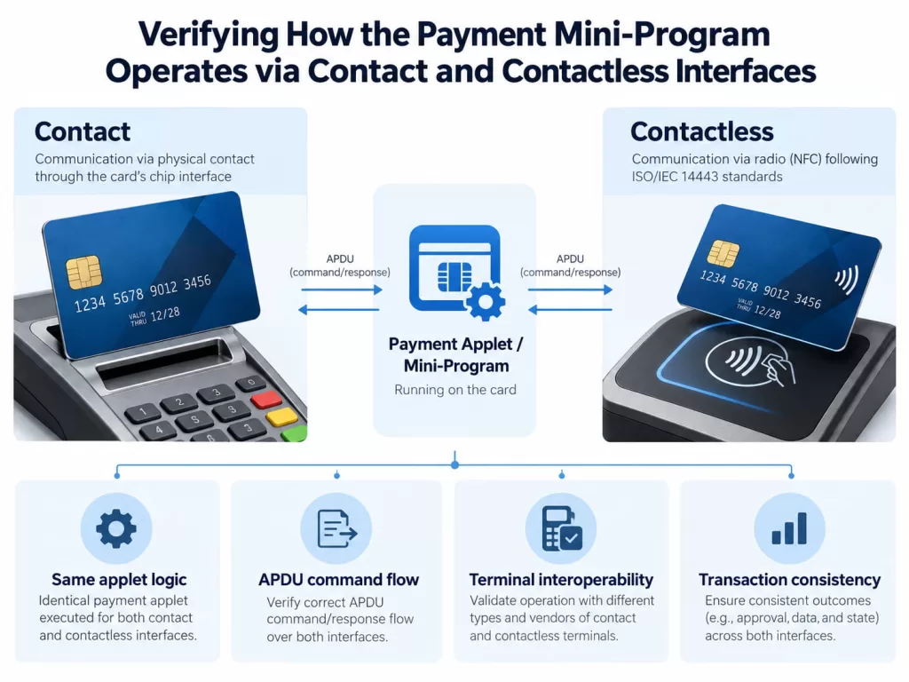
Verifying How the Payment Mini-Program Operates via Contact and Contactless Interfaces
Contact and contactless modes do not necessarily require two separate mini-programs.
In many dual-interface banking application architectures, both interfaces can access the same underlying payment application and personalized account data. The chip provides the physical communication channel, while the payment application determines the commands, transaction paths, and parameters available through each interface. However, this does not mean that contact and contactless processing are identical. Contactless payments have their own unique transaction flows, terminal behaviors, and business processing requirements specific to payment organizations.
Therefore, banks should confirm with the mini-program vendor whether the selected payment application:
- Supports both contact and contactless operating modes;
- Uses generic application parameters or interface-specific parameters;
- Supports the required payment organization profiles;
- Is capable of securely sharing keys and cardholder data between the intended interfaces;
- Has been validated on the selected Java Card platform.
The goal is not merely to find a chip labeled “dual-interface.” A payment Java Card used for dual-interface banking must support the complete software architecture that the issuing institution plans to deploy.
For example, DCCO’s J3R150 chip supports the ISO/IEC 7816 contact interface and the ISO/IEC 14443 Type A contactless interface, and complies with the Java Card 3.0.5 and GlobalPlatform 2.3 standards. The J3R180 is also available as a dual-interface JCOP platform.
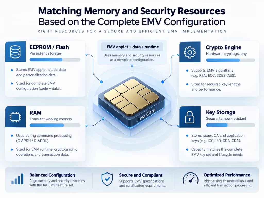
Matching Memory and Security Resources Based on the Complete EMV Configuration
Once the application architecture has been determined, memory becomes the next key selection factor.
No one-size-fits-all answer exists for questions such as whether an EMV application requires exactly 40 KB of memory or whether a bank-grade Java Card must have 100 KB of memory. Actual requirements depend on the payment applet, issuer data, encrypted data, payment scheme configuration, additional applications, and future lifecycle needs.
Calculating Memory Requirements Based on Loaded Bank Applications
Calculate the memory required for a payment Java Card based on the complete set of loaded applications, not solely on the size of the payment applet file.
The actual memory estimate should include the following:
- Payment applet code;
- Personalization data;
- Cryptographic keys and certificates;
- Risk management parameters;
- Additional banking applications or value-added applications;
- Capacity reserved for future updates.
This is critical because a fully personalized payment JavaCard uses more memory than the original application package. During personalization and operation, installed applications may also generate persistent data, security objects, and other resources. Therefore, we recommend verifying available memory only after the payment application and all required data have been fully loaded.
Verifying the Transaction Performance of Java Cards in Actual Payment Environments
Data sheets alone are insufficient to approve dual-interface bank card projects.
While communication speed data reflects interface capabilities, it does not reveal the actual execution speed of a complete payment transaction. Actual transaction duration also depends on application selection, APDU interactions, cryptographic operations, cardholder authentication, terminal behavior, and the payment scheme’s specified transaction workflow.
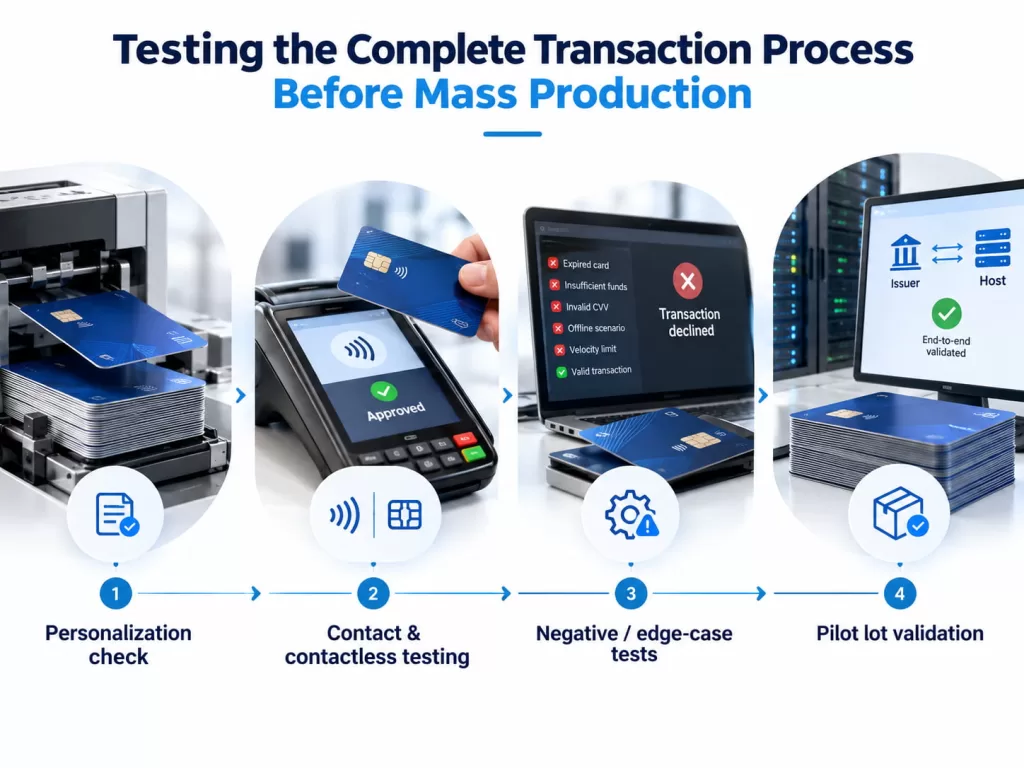
Testing the Complete Transaction Process Before Mass Production
We recommend using actual chips, payment applications, personalized profiles, and typical bank terminals to evaluate transaction performance.
The specific validation process should cover the following steps:
Card activation → Application selection → Payment instruction processing → PIN calculation → Card response → Transaction completion
Because communication environments differ, test contact and contactless interfaces separately.
Card issuers should not focus solely on “what is the maximum communication rate of the chip,” but should measure the following metrics:
- Application selection response time;
- Response time for key payment APDUs;
- Cryptographic processing time;
- Total contact transaction time;
- Total contactless transaction time;
- Performance consistency across repeated transactions and different typical terminals.
Therefore, even if the chip’s technical performance is robust, an unsatisfactory user experience may still result if the payment application, radio frequency (RF) communication, or cryptographic processing causes excessive processing delays.
Selecting the Right Payment Java Card for Dual-Interface Banking Projects
When selecting a payment Java card for dual-interface banking projects, focus on payment applications and authentication requirements.
The specific selection process should follow these steps:
Payment solution → Dual-interface application architecture → Memory → Cryptography → GlobalPlatform → Contact/contactless testing → Certification → Mass production
The J3R150 and J3R180 Java smart cards provide the dual-interface functionality, Java Card runtime environment, application management support, and sufficient memory capacity required for demanding financial projects. However, the final selection should still be based on the bank’s actual application, customization, transaction processes, and certification requirements.
You only need to remember one key principle:
Select a Java card that has undergone full payment platform validation on both interfaces, rather than simply choosing the chip with the largest memory or the fastest nominal communication speed.